Taiwan semiconductor manufacturing (TSMC), a firm that backs huawei, has made a clean sweep of the 5nm process, leaving its rivals with three regrets
In the age of the "national mad chip", imagine the spectacle of 12 million 12-inch wafers lined up. The 3,600-kilometer line, which stretches from Beijing to Lhasa, Tibet, is the world's leading contract wafer manufacturer and the world's largest supplier of logic capacity.
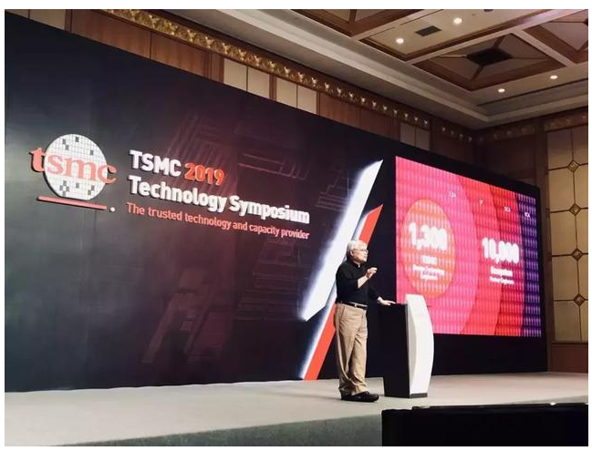
TSMC was held in Shanghai technology BBS for many years, is open to the media for the first time in 2019, although a recent event, huawei let TSMC converge high attention in the industry, but the company did not change the schedule to meet with the media, at the same time, also at the scene of the BBS for huawei and TSMC haisi has opened up a loaf special registration channel, to show attention, spokesman sun again, 'says TSMC has been absorbed in deep tillage technology company, wanted to let you know more about the future of the company's business
Model and technology advantages.

Samsung continues to provoke, TSMC 7 nm with strength to prove the first
Recently, due to its own capacity constraints and other factors, Intel has abandoned the wafer foundry business, focus on good processor chips. Compared with Intel's stumbling development of 10 nm technology in recent years, TSMC has been pushing forward to 10 nm, 7 nm and 5 nm in the technology track.
However, TSMC founder chang chung-mou once said, "never look down upon Intel". Although TSMC has caught up with Intel in technological development, its respect for this "old-timer" is still the same.
TSMC's global success in semiconductors is at its best, but there is still one company that Mr Chang once described as a respectable rival, not far away in geographical terms. That is samsung of South Korea.
In 2019 BBS technology, TSMC President jay wei announced that TSMC is the first semiconductor factory in the world to mass produce 7-nm technology, and the next generation of 5-nm technology has entered the trial production stage, which is expected to be mass produced in 2020.
Zhang xiaoqiang, vice President of business development, emphasized again that TSMC's 7-nm technology entered into mass production in the second year, and was the only semiconductor factory in the world to enter into mass production of 7-nm. The number of customers has been increasing, which is a very successful technology in TSMC's history.
Take turns to play emphasis on 7 nm global leader, is because samsung in two years ago has been claim will be "the first" 7 nm semiconductor factory production, but later samsung even their own processor Exynos 9820 to use 7 nm to production, has been more propaganda to play after 6 nm, 5 nm, 3 nm marketing propaganda, in contrast, says deep tillage technology but not much, TSMC, eat a little stuffy, so take advantage of this technology BBS of our company, be sure to get some emphasis on the service of the "glory".

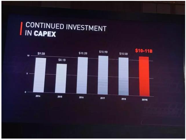
Figure | TSMC has invested us $8 billion to us $10 billion annually for 6 consecutive years to develop advanced technology. (credit: DeepTech)
The 32 - year - old TSMC is the leader in three major campaigns
Over the past five years, TSMC has been spending $10 billion annually and investing heavily on the accelerator all the way. Not only has TSMC become the first semiconductor factory in the world to mass-produce 7-nm technology, but it will also become the first large-scale manufacturer to mass-produce 5-nm technology in 2020, laying its historical position.
How exactly does TSMC stand atop today's global semiconductor giants? There are three key battles that have shaped the semiconductor empire of today in 32 years of history.
The three major battles are: the 0.13 micron technology watershed, the most profitable 28 nm technology legend in history, and the world's first mass production of 7 nm technology to convince Intel.
TSMC was founded in 1987 in an era of IDM factories (design and manufacturing) that included Intel, Texas instruments and MOTOROLA.
However, after chang zhongmou founded the pure wafer OEM mode, he helped qualcomm, broadcom and other large IC design companies to shine, breaking the myth of IDM and opening the era of professional wafer OEM led by TSMC.
Around 2000 was a crucial period for TSMC, when it was still a teenager and naturally not as big as it is today.
At that time, the global semiconductor industry was in the phase of 8-inch to 12-inch wafer, but the investment cost of 12-inch factories was much higher than that of 6-inch to 8-inch factories in 1995. Many IDM factories thought that they could not afford to build 12-inch factories, so they hesitated.
And crucially, 12 "the first process technology is 0.13 micron copper processing technology, compared to the largest competitor umc USES the authorization from the IBM technology, TSMC 0.13 micron copper successfully developed, is pulled open the battle with the key of the distance between the umc, founder of the Nvidia jen-hsun huang said" transform the TSMC 0.13 micron generation!"
The second key battle is the "craziest money-making 28 nm nanoscale technology ever", which has left all competitors, including samsung, far behind. And there is a secret to this process.
At that time, 28 nm HKMG technology was divided into two groups, namely gate-first and gate-last. All semiconductor factories except TSMC adopted gate-first technology following the IBM architecture, while only TSMC adopted gate-last technology.
As a matter of fact, TSMC also adopted gate-first technology at the very beginning, but found that there were insurmountable obstacles in the research and development process, so it took quick internal actions and immediately converted into gate-last technology. After confirmation, 28 nm gate-last technology was defined as the final mass production technology, but the company kept a low profile and kept it secret.
When TSMC released the 28 nm process using gc-last technology, which is different from all semiconductor factories, during an investor presentation meeting, TSMC r&d general jiang shang yi (known as father jiang in the industry) was questioned by foreign legal person about whether gc-first technology was feasible. Or is gate-last technology the answer? Dad jiang said slowly with his usual smile: "now, if we don't argue with you about this, we will know whether the next technology node in the industry will use gate-first or gate-last.
The end of this story, of course, is to make all the competitors regret. By the time everyone finds out that gate-first technology has problems, it will be too late to imitate TSMC to transfer to gate-last technology, because as long as you launch this industry one year ahead of others, almost all the biggest profits will be pocked first.
This 28 nm process made TSMC the most profitable technology in the history of semiconductor industry for 7 to 8 years. It was a legend in the history of semiconductor industry.
If the 0.13 micron technology transformed TSMC, then the 28 nm technology is the key step to make TSMC a global leading semiconductor manufacturer and pave the way for its leading position in semiconductor industry.

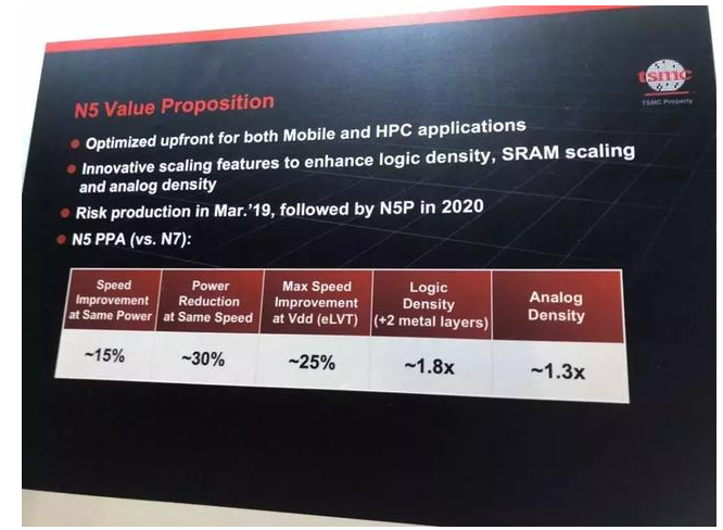
Figure | TSMC 5nm technology will be mass-produced in 2020, targeting two major applications: mobile devices and HPC. (credit: DeepTech)
TSMC's third key battle is the current 7-nm generation. Intel, which had promised to make a big push into the fab industry, began to fade out of the fab industry due to the production difficulties and insufficient capacity of the 10-nm technology, which was expected by chang.
As morris chang once pointed out, "the culture of foundry is to serve customers, but Intel is good at making its own products, and does not have the spirit of serving customers." he has already seen that Intel's corporate culture is not suitable for developing foundry.
Compared with the fading of Intel, samsung has been eyeing the leading position of wafer foundry. With DRAM memory and NAND Flash, the world's leading Flash memory technology, and the backing of branded mobile phones, samsung has been trying to make its way into the fab market with a lot of tricks.
It took TSMC 35 months to go from small production to full production in the 40 nm generation. It took 28 nm to 20 months.
TSMC's lead in the 7-nm and 5-nm technology generations not only puts it ahead of Intel, but also leaves samsung, which has been talking a lot, behind with its "hard power".
Of course, samsung also did not give up to wring hind foot, a few days ago grabbed the Snapdragon 865 processor chip order of 7 nm technology from qualcomm from the hands of Taiwan semiconductor manufacturing co., LTD.

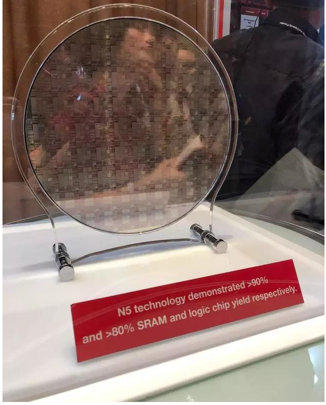
Figure | TSMC shows the world's first 5 nm chip technology strength in Shanghai BBS technology. (credit: DeepTech)
Not only success even more remarkable, the zero excursion, zero defect goal
As the world's biggest foundries, in the technical BBS Wei Zhe home on three strong points in TSMC is technology, the production, don't compete with customers, more shout out to achieve zero excursion, zero defect, zero drift, zero defect) goals, display for the quality requirement is not only successful, but to be remarkable.
TSMC in addition to the world's first mass-produced 7 nm technology, more push forward to adopt the technology of 7 nm plus version, it has entered into 5 nm development, is expected in 2020, and built the entire ecosystem OIP alliance of supply chain, because the world of the semiconductor, rely on leading technology alone is not enough, will also have a more complete and robust ecosystem, to reach the state invulnerable.
It's worth noting that TSMC is currently introducing 6 nm technology, which is using EUV technology as well as 7 nm plus technology.
According to zhang xiaoqiang, the 6 nm process combines the advantages of 7 nm and 7 nm plus technologies, and reduces light masks, bringing customers higher performance and lower cost.
According to the industry, shortly after the mass production of the 7-nm plus version, TSMC will start mass production of the 6-nm technology in 2020. The goal is to quickly update the technology so that samsung can't keep up with the pace.
2019 will be a special year for TSMC. When Mr Chang officially retires in 2018, the first year TSMC will face the "post-mr chang era", it is at this time that TSMC unexpectedly becomes a key player in china-us relations, whose every move is seen in the global technology industry.
TSMC's "hard power" -- including leading 7 - and 5-nm technologies, and starting 3-nm technologies -- has proven itself to be a semiconductor leader, but the industry environment is so volatile that not only does it not want to let up, it needs to tighten the screws.
Pick in the 2019 open technology BBS, foreign reveal the mysterious, low-key veil, "chang era" after TSMC is more different look and feel, to the outside world not only to others cold technology "high, big," image, to let more people understand its business model and corporate culture, let more people into the bibcock, know more about TSMC.
(disclaimer: this article is transferred from the network, the copyright belongs to the original author, if necessary, please contact us to delete)


